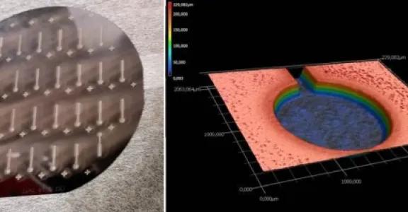
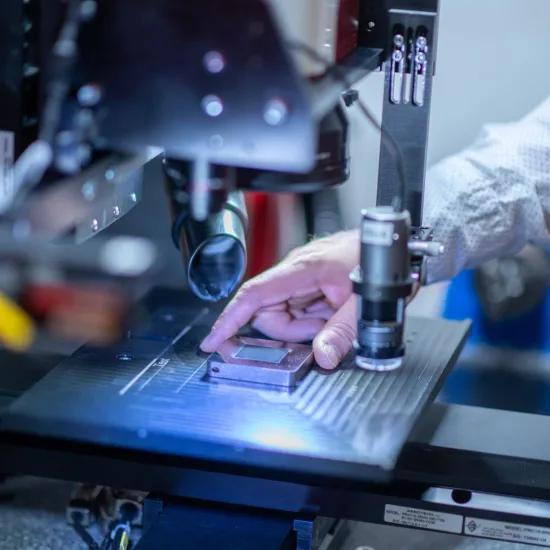
In cooperation with the Swiss CERN, Sirris is evaluating the creation of cooling channels in silicon wafers by means of femtosecond (fs) laser ablation.
Compared to traditional semiconductor fabrication technology ('deep silicon etching'), femtosecond laser technology offers a number of advantages:
- It is not necessary to use a mask (litho step), it's all about direct writing. It is therefore easy to change the design of a channel: this requires only software programming, not hardware masks.
- The traditional silicon etching process is based on SF6, a greenhouse gas that is not needed in fs lasering.
- Due to strong advances in laser technology, the process is competitive in terms of speed and cost for silicon wafers.
On the other hand, a lasered surface is rougher than an etched surface and the effect of this has to be investigated.
In this preliminary study, channels for coolant are lasered and it is shown that you can close these channels again by means of wafer-to-wafer bonding. This cooling is used to stabilise the temperature of detectors used in CERN's experiments.
(Image above: left: a 4-inch wafer with lasered test structures; right: a microscope image of a structure)


