The Internet of Things is conquering the world, already well established in some domains and starting a revolution in others, such as the medical and patient care sector. The new upcoming applications may require other integration techniques to be considered. Enter '3D-PID', developed by Sirris, offering a great flexibility and capacity for customisation, as the approach is essentially based on 3D printing techniques. Discover the four steps of this approach and its advantages here!
Context
The integration of intelligence in products has been a fast growing trend for several years. The addition of sensors that generate and communicate data remotely is already common practice in application areas such as predictive maintenance, automotive, environmental monitoring or industry 4.0.
Recently, new sectors have emerged that can make use of devices that, specifically or even in addition to a main mechanical or structural function, can detect an environmental or event stimulus and communicate it. The Internet of Things (IoT) is this new ecosystem to be reckoned with. Now, even the smallest household appliance can be equipped with intelligence and communication capabilities, and the upcoming arrival of new e-health or remote diagnosis protocols will revolutionise the medical and patient care sector.
Detecting and communicating information, and thus generating data that can be used at a higher level (software), first of all implies having devices (hardware) equipped with functionalised transducers, signal acquisition and shaping stages, as well as remote communication means, not to mention energy management. Many electronic solutions exist to ensure all these functions. Their integration is usually done in the form of Printed Circuit Boards (PCBs), rigid or flex, integrated in a protective packaging.
But the new applications that are coming up require other integration techniques to be considered, also driven by considerations related to the circular economy (facilitating recycling and/or remanufacturing, using biosourced, biodegradable or recycled materials), security (single-use detection heads combined with reusable electronics) or miniaturization (discrete integration, management of micro-samples, reduced energy consumption).
Plastronics and 3D-PID
The term 'plastronics' refers to the marriage between the use of plastics and electronics. This technological approach aims to meet the new needs mentioned above, by allowing the integration, without PCB, of electronic functions and components directly on substrates and other structural elements (3D packaging) made of polymer materials.
Strongly driven by latest developments in printed electronics, this approach is the basis of recent innovative integration techniques such as IMSE (In-Mould Structural Electronics) or 3D-MID (3D-Moulded-Interconnect-Device).
The principle of 3D-PID, 3D-Printed Interconnect Device, developed by Sirris is inspired by these last two concepts, but offering a much greater flexibility and capacity for customisation, as the approach is essentially based on 3D printing techniques.
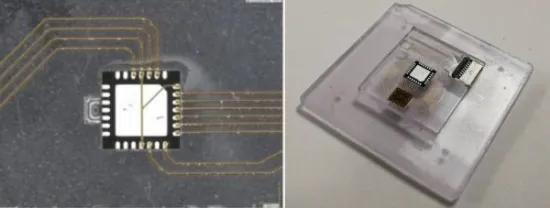
Figure 1 - PCB-less integration and interconnection of electronic components in 3D printed substrates (3D-PID)
3D-PID approach developed by Sirris
The integration of electronic components on/into polymer substrates according to the 3D-PID approach developed by Sirris, consists of four main steps:
- From the electronic function to be fulfilled, a first design is made according to a conventional design for general purpose electronics. After selecting the necessary components (sensors, microcontrollers, resistors, capacitors, active integrated circuits), a schematic is drawn in a standard electronic design software. This schematic is composed of the various interconnections necessary to build the required logic.
- Then, the physical layout of the different components as well as the layout of the conductive tracks needed to interconnect the different chips is defined. The components must be treated as if they were located on the bottom side of a conventional board. Indeed, one of the particularities of the 3D-PID approach is that it integrates the chips upside down in the 3D printed substrates, in order to make the interconnection on the pads which are then on the same level as the main surface. Based on this, the routing can begin. This step is one of the most crucial in the process. Due to the impossibility of using vias, ground planes or multiple layers, the crossing of the tracks is achieved through a dielectric resin distributed between each 'layer' at the crossing point.
- Then, the substrate to be 3D printed is modelled according to the electronics to be integrated, the circuitry ensuring the interconnection, as well as the primary functionality of the board. The next action consists in dimensioning the cavities in the future structure to be 3D printed, by integrating the necessary clearances, but also the flow areas for the resin which will be in charge of ensuring the mechanical resistance and the structural continuity between the surface of the substrate and the connection pads of the electronic components.
- Based on this design, we can proceed to the actual implementation steps with sequentially:
-
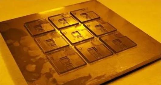
- The realisation of the polymer substrate by 3D microprinting (Figure 2)
Figure 2 - Substrates by 3D microprinting
-
- Integration of electronic components in the substrate and their micro-encapsulation by selective deposition and curing of resin
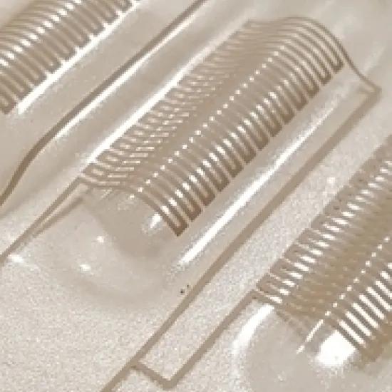
- Printing of the circuitry by selective micro-deposition and sintering of conductive and dielectric inks (Figure 3)
Figure 3 - View (3D optical microscope) of the final circuit, including crossover areas (left) and detail of the micro-printed circuitry in a substrate-component transition area
-
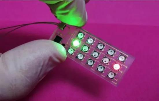
- A last 3D printing step allows, if necessary, to finalise the structural part of the substrate, and to protect the printed tracks (Figure 4).
Figure 4 - Complete and functional 3D-PID component with SMD components integrated on a 3D printed substrate and fed through micro-printed gold circuitry
Advantages of 3D-PID
This 3D-PID approach, based solely on 3D micro-printing techniques, is the solution for integrating electronics into plastic parts that offers the greatest flexibility and the greatest capacity for customisation, compared to other 3D plastronic techniques available on the market. It is compatible with very small series, even unitary.
This research was conducted with the support of the Service Public de Wallonie (Direction générale de l'Emploi, l'Économie et la Recherche) and the EU-MANUNET programme (EMMA project, MNET19/NMCS-3661), in collaboration with Gruppo Pro Logic and VOCSens.


